 |
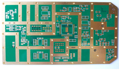
层数/Layers:4-Layers FR4 (RO4350B) 板厚/Thickness: 1.0mm 最小孔径/Min.Hole Size: 0.20mm 线宽线距/Width/Space:4.0/4.0mil 表面处理/Surface Treatment: ENIG 特殊工艺/Special Process:Impedance Control 应用领域/Appilcation:Microwave/Sensors |
High Frequency PCB
High Frequency PCB or calls Microwave PCB / Radio Frequency PCB/RF PCB are widely used in wireless communications,wireless networks and satellite communications, in particular the popularity of 3G networks exacerbate the market demand for the product on the High Frequency PCB.Today, the demand for Microwave material PCB (Quick turn around PCB) design is on the rise, Access to wireless high speed (high frequency) data is quickly becoming a necessity in multiple markets like Defense、Aerospace and Mobile Networks. Evolving market needs continue to drive forward development of High Frequency printed circuit board. like 50+ GHz microwave radios or defense airborne systems, also it can meet Halogen Free PCB together.


